





Sorry, no sales person is available right now to take your call. Pls leave a message and we will reply to you via email as soon as possible.
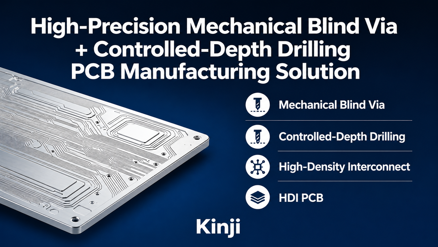
High-Precision Mechanical Blind Via + Depth-Controlled Drilling PCB Manufacturing Technology Solution
2026-07-20
【Industry Background and Pain Points】
The PCB industry is currently accelerating its evolution toward High-Density Interconnect (HDI), particularly in niche sectors such as 5G millimeter-wave RF modules, automotive LiDAR signal processing boards, and medical imaging front-end acquisition cards. These applications commonly require multi-layer fine interconnections within limited board thicknesses. While traditional laser-drilled blind vias offer high precision, they entail significant equipment investment and high per-board costs. Conversely, conventional mechanical drilling struggles to consistently control blind via depth (often resulting in breakthrough or failure to reach the target layer), leading to yield degradation and design re-spins. According to industry surveys, over 37% of HDI projects experience extended prototyping cycles or are forced to adopt higher-tier processes due to substandard blind via fabrication, significantly delaying product time-to-market. In this context, mechanical blind via + depth-controlled drilling technology—offering a balance of precision, stability, and cost-effectiveness—has emerged as a critical differentiator for mid-to-high-end HDI applications.
【Product Core Specifications】
Kinji's mass-production-grade mechanical blind via + depth-controlled drilling PCB supports a minimum blind via diameter of 0.15 mm (corresponding to drill bit specification Φ0.15 mm), with hole position accuracy of ±0.05 mm and depth control tolerance strictly maintained within ±25 μm (measured CPK ≥ 1.33). It reliably achieves arbitrary adjacent-layer blind via structures such as L1-L2, L2-L3, and L3-L4. The solution supports a standard 6-layer stack-up (including 2 blind via layers + 1 buried via layer), with dielectric layer thickness compatibility ranging from 30 to 120 μm. Surface finishes include ENIG, Immersion Silver, and OSP. Blind via inner wall roughness Ra ≤ 0.8 μm, ensuring uniform subsequent copper plating filling and signal integrity. Compared with the industry-standard depth control tolerance of ±50 μm, this process improves precision by a factor of two, approaching the level of some laser-drilled blind vias, while reducing costs by approximately 40%.
【Core Competency Analysis】
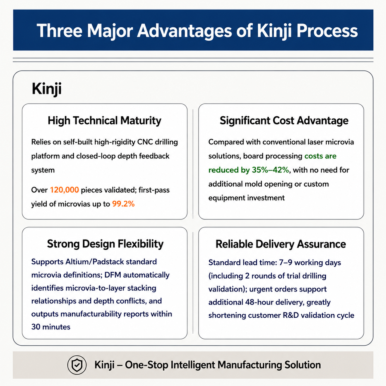
Kinji's process offers three key differentiated advantages: First, high technological maturity—built upon an in-house high-rigidity CNC drilling platform and a closed-loop depth feedback system, it has been validated through cumulative mass-production runs exceeding 120,000 boards, achieving a first-pass yield of 99.2% for blind vias. Second, significant cost benefits—compared with equivalent laser blind via solutions, per-board processing costs are reduced by 35%–42%, with no additional mold-opening or customized equipment investments required. Third, strong design-friendliness—it supports standard blind via definition formats for Altium/Padstack, and the DFM (Design for Manufacturing) tool automatically identifies blind via layer stack relationships and depth conflicts, delivering a manufacturability report within 30 minutes. Fourth, reliable delivery assurance—standard lead time is only 7–9 working days (including two trial-drill validations), while expedited orders support 48-hour rush delivery, greatly shortening customers' R&D validation cycles.
【Typical Application Scenarios】
In 5G Massive MIMO antenna array baseband boards, this process successfully achieved low-inductance blind via connections between the L1-L2 RF routing layer and the L3 power layer, effectively suppressing resonance interference, with measured insertion loss reduced by 1.8 dB @ 28 GHz compared with conventional through-holes. On industrial-grade high-precision Σ-Δ ADC acquisition boards, L2-L3 depth-controlled blind vias precisely connect the reference ground plane to the analog sensitive area, boosting PSRR by 8 dB and stabilizing SNR at 112 dB. In Mini-LED backlight driver PCBs, L4-L5 micro-blind vias enable a direct thermal dissipation path between the IC thermal pad and inner-layer copper foil, reducing junction temperature by 9.3°C under a current density of 120 mA/cm², significantly extending LED module lifespan.
【Selection Recommendations and Outlook】
It is recommended that customers prioritize this solution under the following conditions: blind via depth ≤ 120 μm, target-layer dielectric thickness deviation ≤ ±10 μm, blind via count per board < 5,000, and for mid-volume HDI projects where cost and lead time are sensitive. Looking ahead, as emerging applications such as AI server CXL interconnect boards and AR glasses optical positioning modules drive demand for "asymmetric stack-ups + selective blind vias," Kinji will continue to upgrade its depth-control algorithms and multi-axis coordinated drilling capabilities. It plans to launch a next-generation process platform in Q2 2026 supporting 8-layer stack-ups, ±15 μm depth control tolerance, and contoured blind via shapes, further expanding the application boundaries of mechanical depth-controlled drilling in advanced packaging substrates and Chiplet interconnect carriers.
trending news
Contact Us