





Sorry, no sales person is available right now to take your call. Pls leave a message and we will reply to you via email as soon as possible.
HDI PCB vs. Standard PCB: Key Differences and Advantages
2026-08-18
Printed Circuit Boards (PCBs) serve as the core framework of electronic systems, undertaking dual responsibilities of mechanical support and electrical interconnection. From everyday smartphones and automobiles to aircraft and deep-space rockets, PCBs are ubiquitous and continuously drive technological innovation in cutting-edge fields such as aerospace. Admittedly, conventional PCBs have acted as the cornerstone of the industry for decades. However, market demand for smaller, faster and higher-performance products has fueled the rise of High-Density Interconnect (HDI) technology. Although both types of PCBs share fundamental functions, they differ markedly in design complexity, manufacturing processes, stack-up architecture, cost structure and application scenarios. This article systematically sorts out their distinctions, respective strengths, existing challenges and applicable fields, and provides reference for material selection.
1. What Is a Standard PCB?
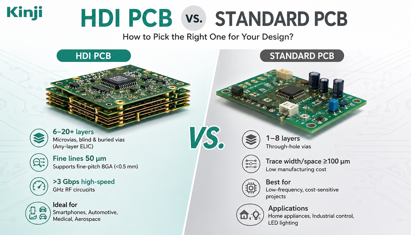
A standard PCB, also known as a conventional PCB, is the most widely adopted solution in electronic circuits. It features relatively simple designs, generally adopting FR-4 glass fiber substrates laminated with copper foil circuits. The number of layers can be flexibly configured according to requirements, with typical products ranging from 1 to 8 layers, commonly including single-sided, double-sided and multi-layer hybrid structures. While standard PCBs can be fabricated with 12 layers or more, their cost-effectiveness declines sharply as layer count increases. Hence, designs requiring higher layer counts usually turn to HDI solutions.
Such circuit boards rely on mechanically drilled through-holes for interlayer connection, with relatively generous trace widths and spacings, generally above 100 μm. Benefiting from its simple structure, standard PCBs boast core merits: low manufacturing costs, short lead times, and proven long-term market reliability. Therefore, they are widely applied in consumer electronics, industrial controllers, automotive subsystems, LED lighting, entry-level PCs, household appliances, toys and other sectors, achieving a favorable balance between cost and performance.
2. What Is an HDI PCB?
HDI PCBs are engineered to integrate maximum functional units within an extremely compact layout, and have become the core support for high-end electronic systems. HDI technology greatly improves circuit board integration capacity — its streamlined, high-density designs easily accommodate complex stack-ups of 6, 10, 20 layers or even more. The breakthrough hinges on the sophisticated adoption of advanced interconnect structures including microvias, blind vias and buried vias, which gradually replace traditional through-holes. This not only enables more precise component placement, but also significantly optimizes signal routing efficiency.
Classification of HDI Grades
· 1st-order HDI: Laser microvias only connect the outer layers with adjacent inner layers; relatively simple process, entry-level HDI solution.
· 2nd-order HDI: Two laser drilling procedures, with staggered or stacked microvia structures enabling deeper interlayer connections.
· 3rd-order HDI: Three laser drilling processes with more complex microvia structures and higher wiring density.
· Any-layer Interconnect (Any-layer / ELIC): Direct interconnection between every layer via microvias, the ultimate form of HDI delivering maximum wiring density at the highest production cost.
Typical characteristics of HDI boards include extremely compact trace widths and spacings. Mass production capability normally reaches 75 μm, and advanced processes can further scale down to 50 μm or finer, realizing ultra-high wiring density and superior electrical performance. In terms of materials, HDI adopts high-performance FR-4 or Rogers high-frequency laminates with specially optimized dielectric properties to guarantee signal integrity under high-frequency and high-speed transmission conditions.
Its advantages are evident: shorter interconnection paths, lower signal attenuation and greater design flexibility. Whether for tablets, smartphones, medical instruments, automotive electronics or aerospace equipment, HDI PCBs achieve miniaturization without compromising electrical performance or long-term reliability.
3. Key Differences Between Standard PCB and HDI PCB
| Comparison Dimension | Standard PCB | HDI PCB |
| Wiring Density | Relatively low; trace width/space generally ≥ 100 μm | Ultra-high; trace width/space down to below 75 μm, advanced processes reach 50 μm |
| Typical Layer Count | 1–8 layers (economical range); up to 12+ layers with rising costs | 6–20+ layers; any-layer structures support higher layer counts |
| Via Types | Mainly mechanically drilled through-holes | Combination of microvias, blind vias and buried vias (laser drilling) |
| Substrate Grade | Standard FR-4 | High-performance FR-4 or Rogers high-frequency materials |
| Manufacturing Process | Conventional mechanical drilling + lamination | Laser drilling + sequential lamination + multiple pressing cycles |
| Signal Integrity | Suitable for low-frequency/low-speed signals (<1 Gbps) | Optimized for high-frequency/high-speed signals (>3 Gbps) |
| Fine-pitch BGA Support | Difficult to support pin pitch below 0.65 mm | Supports pin pitch below 0.5 mm and even finer pitches |
| Typical Applications | Home appliances, industrial control, LED lighting, entry-level electronics | Smartphones, tablets, automotive electronics, communication equipment, aerospace |
4. Core Advantages of HDI PCB
Miniaturization and improved electrical performance are two major strengths that make HDI PCB superior to traditional designs. Leveraging thin dielectric cores and multi-layer stack-up technology, HDI integrates more circuits and active/passive components within a limited area. Laser-drilled microvias enable efficient three-dimensional interconnection. In some designs, passive components can even be embedded inside the board to further free up surface space.
In terms of signal integrity, HDI technology delivers excellent impedance control to safeguard high-speed digital and RF systems. Equivalent capacitance embedded in thin dielectric layers, precise trace alignment and fine line dimensions collectively optimize frequency response and effectively suppress crosstalk. When standard PCBs fail to meet stringent design targets due to routing bottlenecks or signal degradation, HDI can often provide a reliable, high-performance integration solution.
Furthermore, the compact size of HDI reduces board footprint, freeing up more space for batteries or other functional modules. This advantage is particularly prominent in smartphones, wearable devices and aerospace payload design.
5. Challenges of HDI PCB
Despite outstanding strengths, HDI PCB also faces notable challenges. Its manufacturing relies on precision processes such as laser drilling and sequential lamination, greatly increasing production complexity. Meanwhile, requirements for specialized equipment and strict process control push up overall fabrication costs.
Thermal management constitutes another major bottleneck. High-density layouts reduce component spacing and intensify thermal coupling. Thin dielectric layers restrict copper thickness and heat dissipation channels, often requiring thermal simulation, thermal via arrays or external cooling devices for temperature control. Engineers must pay close attention to signal integrity and power integrity during high-speed circuit design. Minor impedance discontinuity or power noise may lead to closed eye diagrams or increased bit error rates for high-speed interfaces, making routing highly technically demanding.
In addition, HDI production imposes extremely strict requirements on precision and reliability verification. Manufacturers need precision laser drilling equipment, Automated Optical Inspection (AOI), flying probe testing and other capabilities. Factories without a complete advanced process system are often unable to undertake such projects.
6. When to Choose HDI PCB Instead of Standard PCB
The selection between HDI and standard PCB hinges on design priorities and cost budgets. Below is the selection guideline:
Scenarios where HDI is recommended
· Component pin pitch below 0.5 mm (e.g., fine-pitch BGA, CSP packages)
· High-speed digital interfaces exceeding 3 Gbps (DDR4/DDR5, PCIe Gen3 and above, USB 3.0/3.1, HDMI 2.0, etc.)
· RF/microwave circuits operating at GHz frequency bands
· Strict size and weight limits for end products (wearable devices, drones, aerospace payloads)
· High-density multi-layer routing required with more than 12 layers
Scenarios suitable for standard PCB
· Operating frequency below 1 Gbps with slow signal edge rates
· Component pin pitch ≥ 0.65 mm, mainly through-hole components or large-pitch SMD
· Ample board space with no special miniaturization requirements
· Cost-sensitive product budgets
· High reliability requirements without high-frequency/high-speed performance demands
In industries such as communication infrastructure, automotive electronics, medical equipment and aerospace, where high performance and miniaturization are mandatory, HDI has become an irreplaceable design foundation thanks to its compact layout and excellent signal retention capacity. Standard PCBs, by contrast, maintain a solid market position in household appliances, industrial control equipment and entry-level electronics by virtue of cost efficiency, proven reliability and production convenience.
Conclusion
HDI PCBs and standard PCBs are both indispensable basic interconnection components for electronic systems, yet they occupy distinctly different positions. Standard PCBs remain a trustworthy option for low-cost, mid-to-low frequency applications, while HDI PCBs achieve breakthroughs in miniaturization, high-speed transmission and high-density integration. The final choice depends on specific application demands: HDI fits advanced compact systems, and standard PCBs are better suited for cost-oriented simple designs.
Whether you opt for mature and reliable standard PCB solutions or high-end HDI to achieve high performance and miniaturization goals, Kinji Group delivers one-stop services covering engineering design, rapid prototyping and mass production. The Group boasts mature processes and cost control capabilities for standard PCBs, and reserves special technologies including high-frequency hybrid lamination and laser drilling for HDI and high-precision boards. We provide high-reliability deliveries for diverse scenarios such as automotive electronics, communications, medical care and aerospace.
trending news
Contact Us