

Sorry, no sales person is available right now to take your call. Pls leave a message and we will reply to you via email as soon as possible.
IC Substrate Classification: Processes, Materials, Applications
2025-11-17
Introduction
IC substrates, also known as packaging substrates, are critical components in semiconductor packaging. They provide mechanical support, electrical interconnection, and thermal management for integrated circuits. Understanding their classification by process, form, material, and application helps clarify technology roadmaps, material selection, and market positioning.
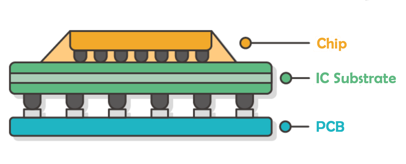
Figure 1. IC Substrate Structure Diagram
1. Classification by Packaging Process (Chip-to-Substrate Interconnection)
Wire Bonding (WB)
Process Characteristics: The chip is placed face-up, and gold or copper wires connect the chip pads to substrate traces. Typical Packages: WB-BGA, WB-CSP, RF Modules. Applications: RF modules, memory devices, MEMS, mid-to-low-end PMICs.
Flip Chip (FC)
Process Characteristics: The chip is placed face-down, with solder bumps or micro-bumps directly connecting to substrate pads. Enables high-density, high-performance interconnections. Typical Packages: FC-BGA, FC-CSP, FC-LGA. Applications: CPUs, GPUs, high-end application processors (AP), high-speed interface chips.
Embedded Die (ED) Packaging
Process Characteristics: Chips are embedded within substrate layers before lamination. Laser drilling and electroplating redistribute connections. Compact structure with reduced thickness. Typical Packages: Embedded Die BGA/CSP, Embedded SiP. Applications: Ultra-thin PMICs, RF front-end modules, wearable/IoT SiP, SSD controllers.
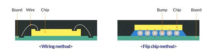
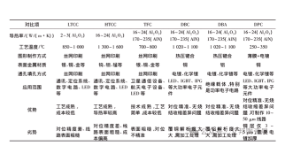
Figure 2. Comparison of IC Substrate packaging processes
2. Classification by Packaging Form (Product Type)
- BGA (Ball Grid Array): Includes FC-BGA and WB-BGA, widely used in processors and high-performance chips.
- CSP (Chip Scale Package): FC-CSP and WB-CSP, suitable for memory and mobile SoCs where space is critical.
- RF Module Packaging: Designed for RF front-end modules in communication devices.
- PGA/LGA (Pin/Grid Array): Used in servers and high-performance computing requiring reliable electrical connections.
3. Classification by Substrate Material
- Rigid Substrates Materials: BT resin, ABF resin, MIS. Features: High mechanical strength, mature processes, suitable for mid-to-high-end packaging.
- Flexible Substrates Materials: Polyimide (PI), Polyester (PE). Features: Lightweight, bendable, ideal for wearables and flexible electronics.
- Ceramic Substrates Materials: Alumina (Al₂O₃), Aluminum Nitride (AlN), Silicon Carbide (SiC). Features: Excellent thermal stability and insulation, used in aerospace, defense, and high-reliability applications.
4. Classification by Downstream Application
- Memory Substrate: For DRAM, NAND Flash packaging.
- RF Module Substrate: Applied in 5G communication and smartphone RF front-end modules.
- Processor Substrate: Serves CPUs, GPUs, AI chips, and other high-compute devices.
- MEMS Substrate: For sensors and micro-actuators.
- High-Speed Communication Substrate: Used in data centers, optical modules, and switches requiring high-speed signal transmission.
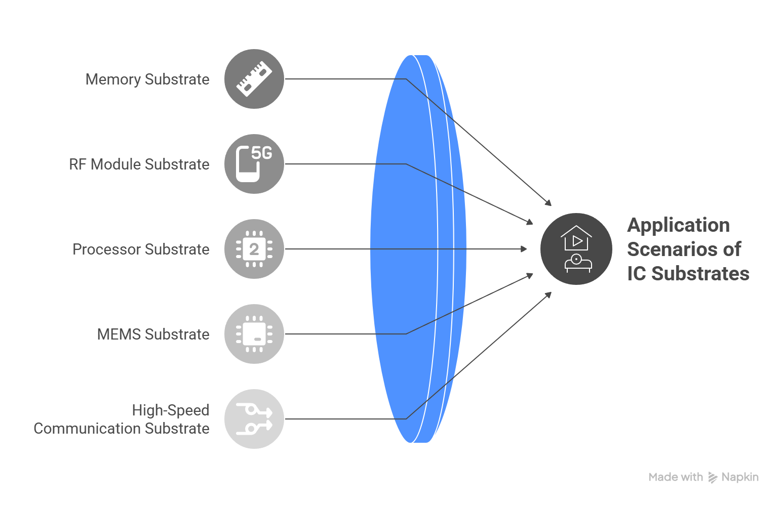
Figure 3. Application Scenarios of IC Substrates
Summary Table
| Classification Dimension | Main Types |
|---|---|
| Packaging Process | Wire Bonding (WB), Flip Chip (FC), Embedded Die (ED) |
| Packaging Form | BGA, CSP, RF Module, PGA/LGA |
| Material Type | Rigid Substrate, Flexible Substrate, Ceramic Substrate |
| Application Field | Memory, RF, Processor, MEMS, High-Speed Communication |
Conclusion
Through multi-dimensional classification, IC substrates can be systematically understood in terms of technology routes, material choices, and application markets. This provides clear guidance for semiconductor packaging design, product selection, and industry development.
Previous Article: PCB Stator Technology for Next‑Gen Electric Drive Design
trending news
Contact Us