
Sorry, no sales person is available right now to take your call. Pls leave a message and we will reply to you via email as soon as possible.
Glass Substrates Driving Advanced Semiconductor Packaging
2025-11-07
Introduction
As advanced packaging reshapes the semiconductor industry, glass substrates are emerging as a critical solution for high‑density interconnects, high‑frequency signal integrity, and cost‑effective manufacturing. Their unique material properties such as ultra‑high flatness, low CTE matched to silicon, and excellent insulation—make them a foundation for next‑generation chip design.

Figure 1. Comparison between Organic Substrate and Glass Core Substrate structures
Performance Advantages and Application Scenarios
Glass substrates are not only stable carriers but also performance enablers. Their dielectric stability and mechanical reliability allow finer routing, higher integration, and improved yield.
- Chiplet/SiP & AI/HPC: Extreme flatness and dielectric stability enable high‑density interconnects and high‑bandwidth memory integration, supporting advanced compute chiplets.
- Silicon Photonics & CPO: Optical transparency and low‑loss characteristics support efficient photonic transmission and co‑packaged optics, reducing signal loss in next‑generation optical interconnects.
- RF & Communication: Stable dielectric constant and low loss factor maintain signal quality from GHz to THz, making glass substrates suitable for RF modules and antenna packaging.
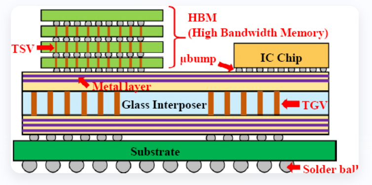
Figure 2. Chip stacking structure: HBM, IC chips, and glass interposer
Manufacturing Paradigm Shift: Panel‑Level Cost Revolution
The industry is witnessing a shift from round wafers to square panels, substantially increasing the number of chips produced per run. This paradigm change is the fundamental driver behind unit cost reductions of 30–40%, enabling glass substrates to scale economically while supporting advanced packaging demands.
To illustrate this transformation, KINJI has developed the Sodium‑Calcium Glass Substrate Board, a double‑sided design with 1.0 mm thickness and 35 μm copper layers. It demonstrates how panel‑level processes can be applied to real products, bridging theory and practice.
Figure 3. Sodium‑Calcium Glass Substrate
Technology Roadmap and Future Outlook
- Near Term (1–3 years): Achieve TGV diameter < 5 μm; aspect ratio (AR) > 10:1.RDL line width/spacing < 2 μm.Establish core processes and complete prototype validation.
- Mid Term (3–5 years): Improve yields in large‑size panel processes. Mature the supply chain and reach cost‑reduction inflection points. Advance standardization of interfaces, materials, and processes.
- Long Term (5+ years): Scale commercialization of CPO and SiPh.Glass substrates become a mainstream solution in 2.5D/3D packaging and optoelectronic integration.
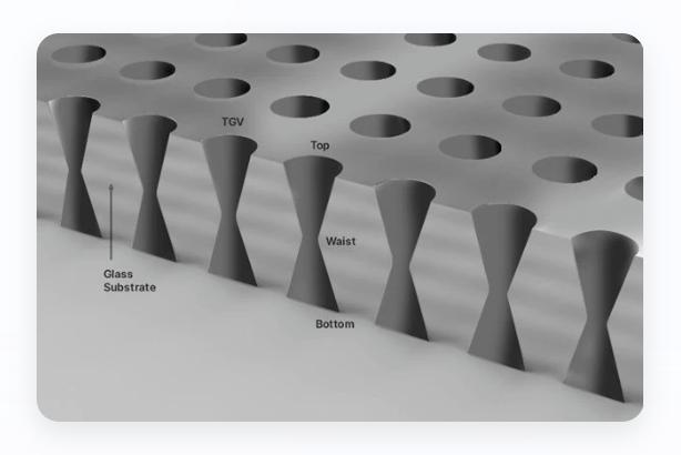
Figure 4. Schematic diagram of Through‑Glass Via (TGV) structure
Conclusion
Glass substrate technology is advancing rapidly as semiconductors embrace advanced packaging. The trajectory is clear:
- Higher density: Finer interconnects on ultra‑flat carriers.
- Signal integrity: Stable dielectric properties and low loss at high frequencies.
- Manufacturing scalability: Panel‑level processes that reduce unit cost.
- Future‑ready architectures: Enabling HBM, silicon photonics, and CPO.
These advances align with the demands of AI, HPC, and data centers—higher bandwidth, lower power, and reliable scale.
KINJI High-Aluminosilicate Glass Substrate Board features single‑sided copper, 1.0 mm thickness and 35 μm copper layers. It is designed for optical interconnects and RF module integration in advanced semiconductor packaging. We also provide customized glass substrate solutions tailored to specific design needs. Contact our engineering team to explore how these substrates can support your next project.
Figure 5. High‑Aluminosilicate Glass Substrate
trending news
Contact Us