
Sorry, no sales person is available right now to take your call. Pls leave a message and we will reply to you via email as soon as possible.
Next‑Generation Optical Module PCB Technology: High Density, High Speed, and Thermal Management
2025-11-06
Executive Summary
Optical module PCB technology is evolving rapidly to meet the extreme demands of AI data centers and high‑speed networks. From 400G to 1.6T, next‑generation optical modules require higher density, advanced materials, innovative thermal management, and new architectures such as CPO. This article explores the core components of optical modules, their classification, the latest PCB technology trends, and the five key challenges engineers face in design and manufacturing.
Optical Modules: Core Components and Classification
Core Components
- Optical devices: Chips (lasers, detectors) and optical elements (lenses, isolators). These define performance and account for 70%+ of cost.
- Circuit section: Signal driving, control, and processing chips mounted on the PCB.
- Structure and auxiliary materials: Housing, pins, connectors — together with circuits, ~30% of cost.
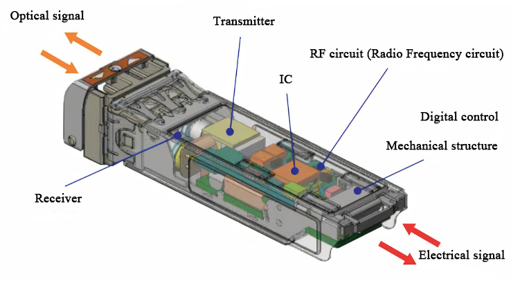
Figure 1. Structure of the optical module
Classification Dimensions
- Form factor: SFP, QSFP, OSFP
- Data rate: 10G, 25G, 100G, 400G, 800G, 1.6T
- Transmission distance: Short (<2 km), medium (10–40 km), long (>80 km)
- Modulation format: NRZ, PAM4, coherent
- Multiplexing: CWDM, DWDM
- Fiber type: Single‑mode, multimode
- Chip material: InP, SiP
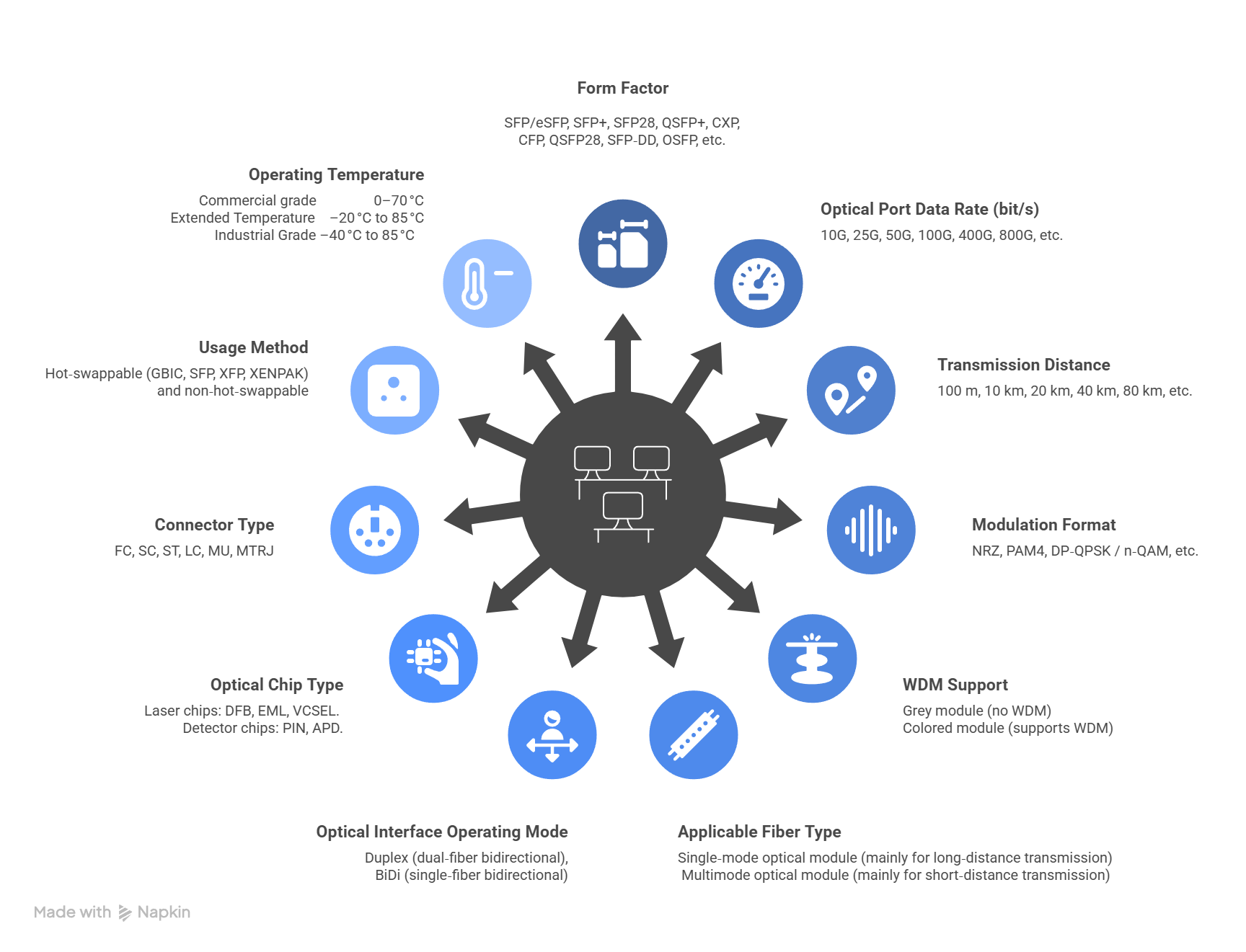
Figure 2. Classification system of optical modules
By Application
- Ethernet modules: Data centers, metro, backbone networks
- Fibre Channel modules: Storage, HPC networks
- Optical interconnects (AOC): Short‑reach (<20 m) server and TOR switch links
- CWDM/DWDM modules: Data center interconnect, carrier networks
- Wireless fronthaul/midhaul/backhaul: Telecom RAN
- Wired access modules: Point‑to‑multipoint telecom access
High‑Speed Optical Module PCB Technology
To support AI data centers and ultra‑high‑speed networks, PCB technology is advancing in five directions: high density, advanced materials, precision processes, thermal management, and new architectures.
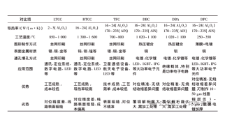
Key Development Trends
| Technology Direction | Current Focus |
|---|---|
| High density & layer count | 400G: ~10 layers; 800G: 12–14; 1.6T: 16+. Line width shrinking from 100 μm to 50 μm (inner) / 75 μm (outer). HDI with blind/buried vias is essential. |
| High‑speed / High‑frequency materials | 400G/800G: M6 laminates; 1.6T: M7–M9 with lower Df/Dk. Goal: Dk < 3.0 composites (e.g., PTFE). |
| Advanced processes | mSAP for finer line widths; ENEPIG/OSP finishes for signal integrity; VIPPO (via‑in‑pad plated over) to increase routing space and improve SI/PI. |
| Thermal management | Liquid cooling for 1.6T+ modules. LCO integrates cold plates into housings. |
| New architectures | CPOintegrates optical engines with switch ASICs, requiring ultra‑dense PCBs, 2.5D/3D packaging, and co‑design. |
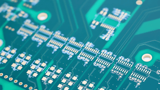
Product Example: 10‑Layer 400G Optical Module PCB
As data rates climb to 400G and beyond, PCB design must balance density, signal integrity, and thermal performance. One proven solution is our 10‑Layer 400G Optical Module PCB, engineered with M6 laminates, precision finishes, and embedded copper blocks to meet these challenges head‑on.
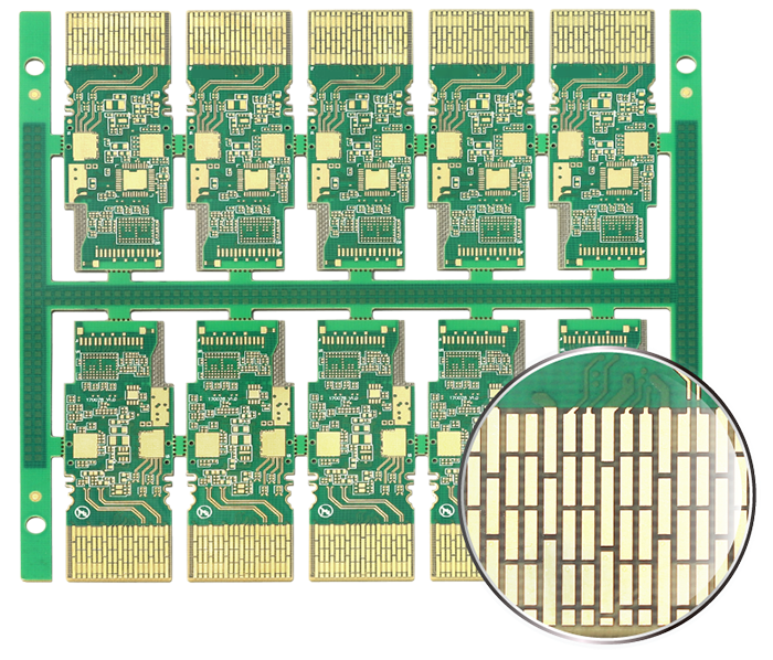
Figure 3. 10‑layer 400G optical module PCB
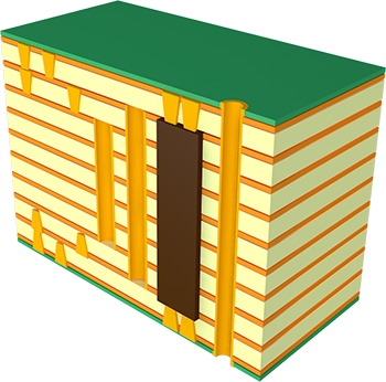
Figure 4. Stack‑up structure of the optical module PCB
Five Core Challenges in High‑Speed Optical Module PCB Design
1. Signal and Power Integrity (SI/PI)
- Challenge: At 224 Gbps/lane, loss, distortion, via stubs, crosstalk, and skew dominate.
- Solution: 3D EM simulation, HDI with laser microvias, low‑Df laminates.
2. Thermo‑Mechanical Reliability
- Challenge: Thin cores, high layer counts, CPO packaging, and liquid cooling stress cause warpage and CTE mismatch.
- Solution: CTE‑matched materials, symmetric stack‑ups, precise lamination/cooling control.
3. Yield vs. Cost
- Challenge: 50 μm lines and 150 μm microvias push subtractive processes to limits, requiring costly mSAP.
- Solution: DFM collaboration, apply premium processes only to critical layers.
4. Design–Manufacturing Disconnect
- Challenge: Late handoff leads to manufacturability and cost issues.
- Solution: Early co‑design with PCB vendors, joint decisions on stack‑up, materials, processes.
5. Validation Risks of New Materials
- Challenge: M7–M9 laminates may lack supply stability, reliability data, or mature processing.
- Solution: Material selection matrices (Dk/Df, Tg, CTE, CAF, cost, lead time); rigorous reliability tests (TCT, HTOL).
Conclusion
High‑speed optical module PCB technology is undergoing rapid innovation. The roadmap is clear:
- Higher density with more layers and finer lines.
- Better signal quality through advanced materials and processes.
- Improved thermal management with liquid cooling and embedded copper.
- Future‑ready architectures via CPO and co‑packaged optics.
These advances aim to meet the ultimate demands of AI data centers: higher bandwidth with lower power consumption.
FAQ
Q1: What PCB materials are commonly used in 400G/800G optical modules?
A: For 400G/800G designs, M6 laminates are widely adopted due to their balance of loss and manufacturability. As speeds move toward 1.6T, advanced laminates such as M7–M9 with lower dielectric loss (Df) and dielectric constant (Dk) become essential. At KINJI, we have hands‑on experience qualifying these materials and can advise on the right choice for your project.
Q2: How can thermal management be ensured in high‑power optical modules?
A: Liquid cooling and embedded copper blocks are now mainstream solutions for 1.6T and beyond. We design PCB stack‑ups that integrate these features while maintaining mechanical reliability. If you’re facing thermal bottlenecks, our engineering team can share proven design approaches tailored to your application.
Q3: What are the main challenges in manufacturability at fine line widths (50 μm and below)?
A: At such geometries, yield and cost become critical. Advanced processes like mSAP and VIPPO are required, but not every layer needs the highest spec. We help clients balance manufacturability and performance by applying premium processes only where they matter most. This design‑for‑manufacturing mindset is part of our daily collaboration with partners.
Q4: Can KINJI support co‑packaged optics (CPO) PCB requirements?
A: Yes. CPO demands ultra‑dense interconnects, 2.5D/3D packaging, and co‑design of optics and electronics. Our team has already supported projects in this space, ensuring signal integrity and thermal reliability at scale. If you’re exploring CPO adoption, contact us to discuss how our expertise can accelerate your roadmap.
trending news
Contact Us