


Sorry, no sales person is available right now to take your call. Pls leave a message and we will reply to you via email as soon as possible.
Planar Transformer Working Principles and PCB Design Guide for High‑Frequency Power Electronics
2025-10-29
What Is a Planar Transformer?
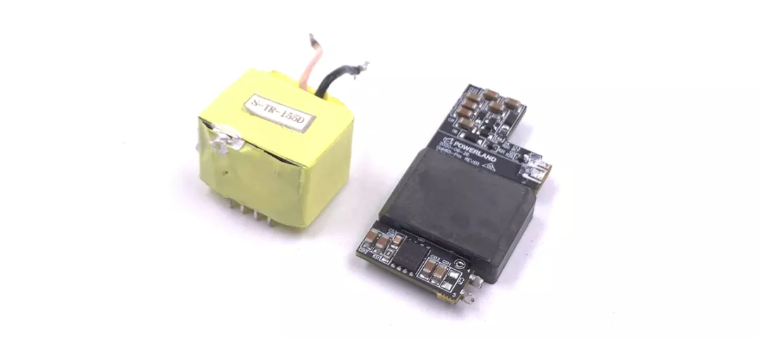
A planar transformer is a high‑frequency magnetic component that uses flat windings and a low‑profile magnetic core. It is designed to meet the demands of modern electronics for higher frequencies, miniaturization, and high power density. Compared with traditional wound transformers, planar transformers differ significantly in structure, performance, and application scenarios.
As a new type of high‑frequency ferrite inductor, planar transformers offer several advantages over conventional high‑frequency transformers:
1. Excellent high‑frequency performance
Suitable for operating frequencies from tens of kHz up to several MHz, with current densities up to 30 A per module, meeting high‑current output requirements.
2. Low leakage inductance and high efficiency
Primary and secondary windings use multilayer PCBs or flat copper strips with tight coupling, minimizing leakage inductance. This reduces switching losses and EMI, improving overall system efficiency.
3. Superior thermal management
The flat structure provides a larger surface‑area‑to‑volume ratio and shorter heat dissipation paths, enabling effective temperature control in high‑power applications.
4. Compact structure, automation‑friendly
Thin, uniform profiles make planar transformers easy to mount on PCBs, supporting power module miniaturization and mass production with high consistency.
5. Flexible and reliable insulation design
Insulation strength can be tailored by adjusting PCB layer count and dielectric thickness to meet safety standards.
Potential challenges:
- Limited number of turns, requiring careful flux control to avoid core saturation.
- Higher parasitic capacitance, which may affect performance at very high frequencies.
- Lower window utilization compared with traditional transformers.
Structural Design of Planar Transformers
Windings and Core Structure
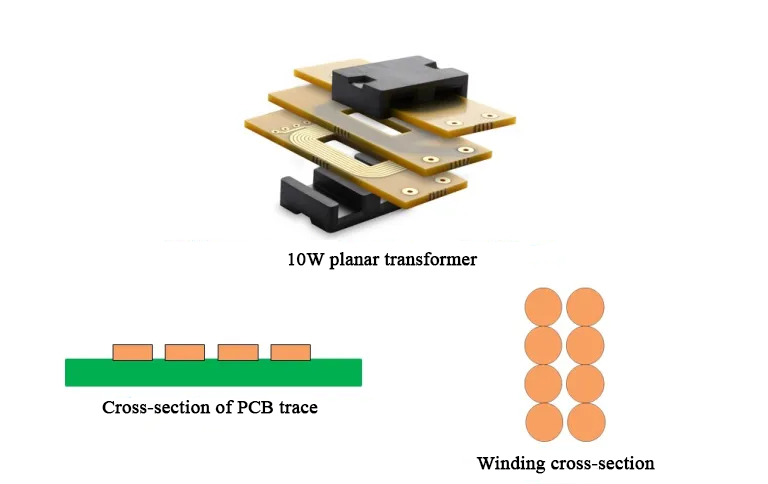
Windings are formed by spiral copper traces on PCBs, with multilayer boards providing interlayer insulation. The magnetic core is mounted in a central window cut into the PCB, typically fixed with tape or metal clamps to complete the magnetic circuit. This design reduces overall height, enabling thin and compact transformer profiles.
Conductor Characteristics and Skin Effect
PCB traces are flat, typically using 1 oz or 2 oz copper. At frequencies below 14 MHz, the skin depth of copper is greater than half the copper thickness. Since most power supplies operate well below this threshold, skin effect losses are negligible, reducing high‑frequency losses.
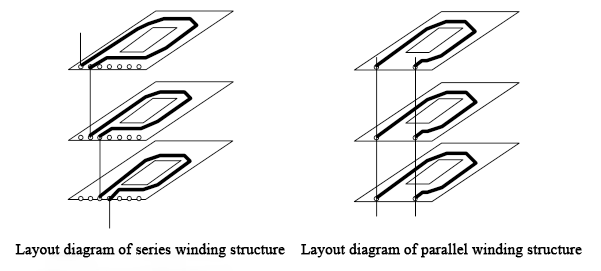
Interconnections between PCB winding layers are achieved through vias, which allow series or parallel configurations to achieve the required turns ratio.
- Series connection: aligned via arrays, with only two vias per layer used to form continuous winding paths.
- Parallel connection: used in low‑voltage, high‑current applications to increase current‑carrying capacity.
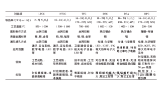
Common Core Types and Characteristics
Planar transformers typically use high‑frequency ferrite soft magnetic materials. Common core types include E, RM, EC, ETD, and EER. Core geometry directly affects winding design, thermal performance, shielding, and power density.
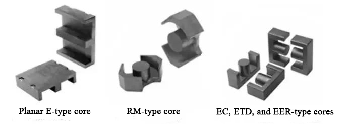
1. E‑type cores
- Advantages: Mature manufacturing, low cost, widely used. Large window area supports wide conductors for high current. Flexible mounting and good thermal performance, suitable for high‑power applications.
- Disadvantages: No self‑shielding; rectangular center post limits winding layout optimization; larger overall size for wide conductors.
2. RM‑type cores
- Advantages: Round center post and edges shorten winding length, reducing copper loss. Compact winding cross‑sections improve coupling and reduce leakage inductance. Better magnetic shielding than E‑type.
- Applications: Where efficiency, space utilization, and EMI shielding are critical.
3. EC / ETD / EER cores
- Advantages: Hybrid between E and RM types. Large window area supports high current, while round center post reduces copper loss and improves winding optimization. Good thermal performance.
- Disadvantages: Like E‑type, shielding is limited.
PCB Design for Planar Transformers
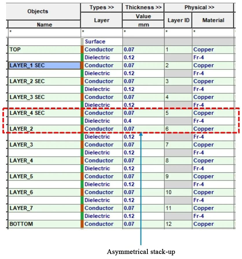
Multilayer Stack‑Up Design
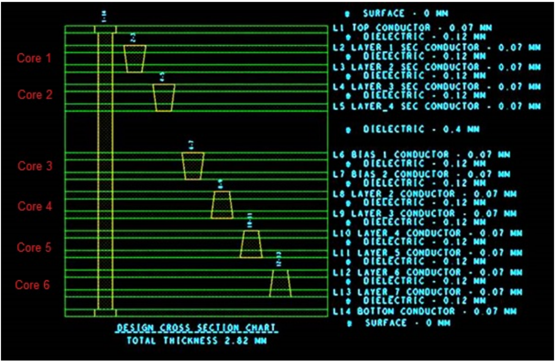
The PCB stack‑up should follow a top‑bottom symmetry principle to balance thermal and mechanical stresses during manufacturing, minimizing warpage and improving yield. Dielectric thickness must meet insulation requirements between primary and secondary windings while maintaining uniform overall thickness for signal integrity and structural reliability.
Copper Thickness and Trace Spacing Guidelines
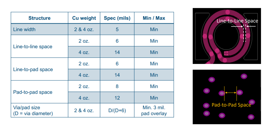
To control cost and lead time, the following design rules are recommended:
| Design Principle | Explanation |
|---|---|
| 1. Material selection | Use manufacturer‑recommended prepregs and cores to ensure stable supply, matched performance, and cost control. |
| 2. Inner copper ≤ 3 oz | Excessive copper thickness increases etching difficulty, line width tolerance, and lamination complexity, raising costs. |
| 3. Minimize blind/buried vias | Avoid unless necessary. For dielectric >0.2 mm, laser drilling is not possible, requiring costly mechanical drilling. |
| 4. Relax board thickness tolerance | Allow ±10% tolerance to reduce lamination difficulty, improve yield, and shorten lead time. |
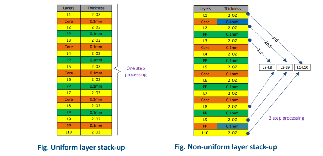
| 5. Single lamination process | Use symmetrical, uniform materials to enable one‑time lamination. Complex stack‑ups requiring multiple laminations increase time and cost. |
Additional recommendations:
- Reduce drilling steps where possible.
- Align vias across layers.
- For buried vias, keep them within adjacent layers (e.g., L2–L3, L4–L5, L6–L7, L10–L11) rather than spanning across multiple cores.
trending news
Contact Us