Sorry, no sales person is available right now to take your call. Pls leave a message and we will reply to you via email as soon as possible.
Alumina Ceramic Substrate
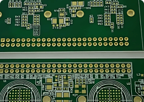
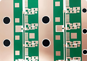
Alumina Ceramic Substrate is a high purity alumina material, sintered at high temperature, with excellent electrical insulation properties, high mechanical strength and wear resistance. Its excellent dielectric constant and temperature stability make it ideal for high frequency applications. Alumina Ceramic Substrates are widely used in electronics, integrated circuits and hybrid circuits, especially for applications that require high performance and reliability. Alumina Ceramic Substrate not only provides excellent electrical properties, but also has good thermal conductivity, which helps to improve the heat dissipation effect of electronic components.
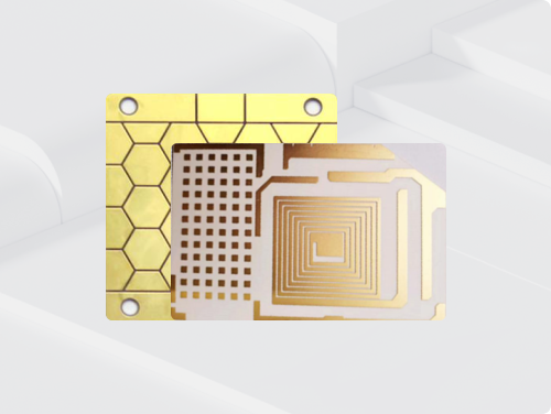
Aluminum Nitride Ceramic Substrate
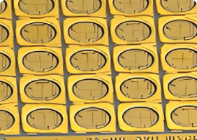
Aluminum Nitride Ceramic Substrate is a kind of high performance Ceramic material with excellent thermal conductivity and low thermal expansion coefficient. It is made of high purity aluminum nitride powder sintered at high temperature and has excellent mechanical strength and resistance. Aluminum Nitride Ceramic Substrates are widely used in electronics, integrated circuits and hybrid circuits, especially for high frequency, high temperature and high power applications, and their excellent thermal management performance helps to improve the reliability and life of electronic components.
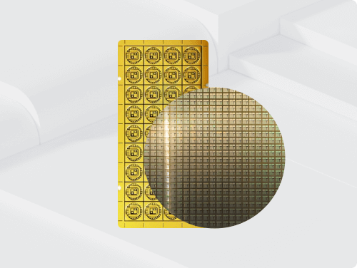
Silicon Nitride Ceramic Substrate
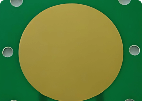
Silicon Nitride Ceramic Substrate, as a new inorganic non-metallic material, has excellent thermal conductivity, insulation and mechanical strength, and is widely used in electronic packaging, semiconductor devices and other fields. Its unique silicon nitride crystal structure gives the substrate excellent thermal shock resistance and chemical stability, significantly improving the reliability and service life of the product. Compared with traditional substrates, Silicon Nitride Ceramic Substrates perform better in high temperature and high-frequency environments, providing an ideal support platform for high-end electronic components, and are favored by the industry.
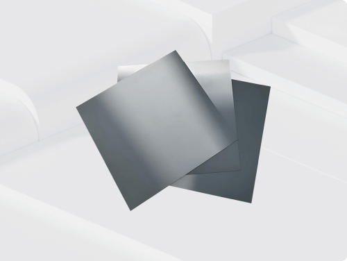
Direct Bonded Copper (DBC) Ceramic Substrate
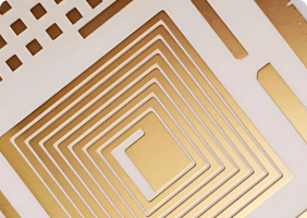
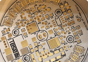
DBC (Direct Bonded Copper) Ceramic Substrate is a high-performance substrate that uses advanced direct bonding technology to tightly bind a highly conductive copper layer to a Ceramic Substrate, achieving excellent thermal conductivity and electrical performance. Its unique structure makes DBC substrates excellent in high temperature, high frequency applications, suitable for power electronics and LED fields. The stability, corrosion resistance and excellent adhesion strength of the DBC Ceramic Substrate provide a reliable platform for high-end electronic packaging, greatly enhancing the performance and attractiveness of the product.
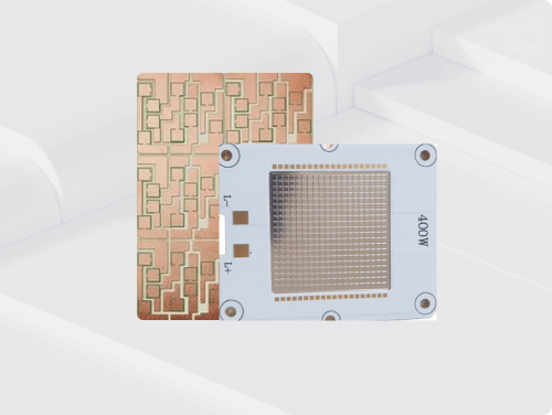
Thick Film Resistance Ceramic Substrate
Thick Film Resistance Ceramic Substrate is a high-performance electronic material that applies thick film resistance technology to ceramic substrate. The substrate has excellent electrical insulation, chemical stability and high temperature resistance, ensuring long-term stability and reliability of the thick film resistance. Its unique thick film technology makes the resistance value have good adjustability to meet the needs of diverse applications. The high performance and excellent machining characteristics of thick film resistance ceramic substrates make them very attractive in power devices and precision electronic components.
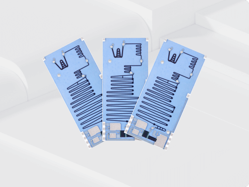
Ceramic Substrate · Hard and Heat Resistant
Ceramic Substrate · Manufacturing Process
-
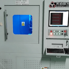
01/Laser Drilling
Using high-precision laser beam to drill precise holes in the Ceramic material. -
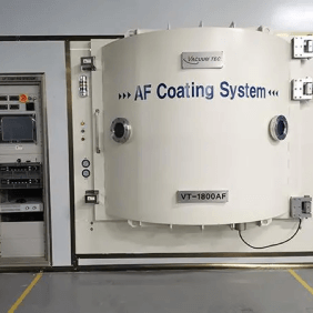
02/Sputtering
In a vacuum environment, high-energy particles bombard metal targets and deposit metal films. -
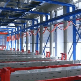
03/Circuits
Precision deposited metal layer, lithographically defined line, etched molding. -
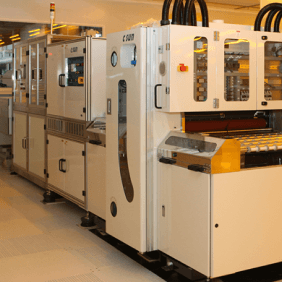
04/Plating
A metal layer is deposited on the Ceramic surface to enhance electrical conductivity and oxidation resistance. -
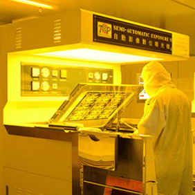
05/Leveling and Polishing
Fine grinding substrate surface to improve flatness and finish. -
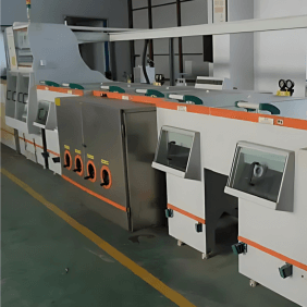
06/Film Removal Etching
Removing the resist layer, the circuit is defined by chemical etching, and the circuit pattern is refined. -
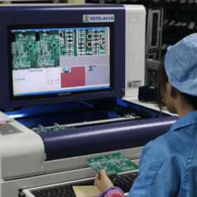
07/E-Test
Check circuit continuity and performance parameters to ensure product performance and quality. -
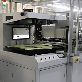
08/Soldermask & Silkscreen
Use solder resistance to protect non-pad areas and print character identification. -
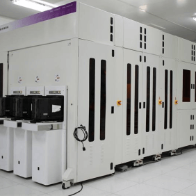
09/Surface Treatment
Cleaning, activation, coating to optimize surface properties and enhance bonding forces. -
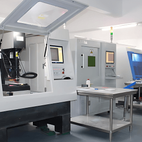
10/Laser Shape
High precision cutting technology for precise cutting of complex shapes ensures smooth edges. -
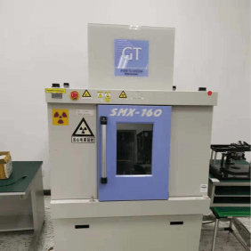
11/FQC & FQA
The final inspection confirms that the product meets the specifications and ensures that the product meets the highest standards before leaving the factory. -

12/Packing & Shipping
It is packaged with anti-static and moisture-proof materials to ensure transportation safety.
Ceramic Substrate · Manufacturing Process
| Item | Unit | Kinji · Ceramic Substrate · Manufacturing Capabilities |
| Maximum Finished Size | mm | 140*190 |
| Numbers of Layers | L | 1 - 6 |
| Board Thickness | mm | 0.2/0.25/0.3/0.38/0.5/0.635/0.8/1.0/1.2/1.5 |
| Minimum Aperture | mm | 0.08 |
| Aperture Taper Tolerance | % | ±30 |
| Minimum Line Width & Line Distance | mm | 0.075/0.040 |
| Surface Treatment | / | Immersion Gold, Immersion Silver, Immersion Tin, OSP, ENEPIG(Ceramic Substrate Can Not Use HASL Technology) |
Ceramic Substrate· Application
