


Sorry, no sales person is available right now to take your call. Pls leave a message and we will reply to you via email as soon as possible.
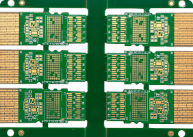
High Reliability · Special Technology PCB · Manufacturer
-
- Heavy copper PCB for automotive
- Layer: 2L
- Board Thickness: 2.0 mm
- Surface Finishing: Immersion gold
-
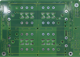
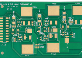
- 4 layer PCB for energy storage mainboard
- Layer: 4L
- Board Thickness: 2.0 mm
- Surface Finishing: LF HASL
-
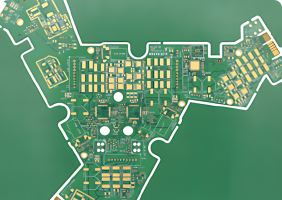
- 6 layer HDI
- Layer: 6L
- Board Thickness: 1.6mm
- Surface Finishing: Immersion gold 2u"
-
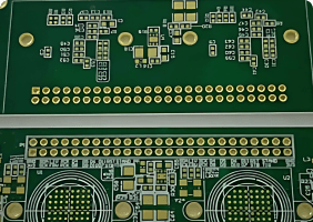
- 8 layer HDI with impedance control
- Layer: 8L
- Board Thickness: 1.6mm
- Surface Finishing: Hard gold plating + Immersion gold
-
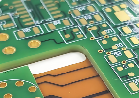
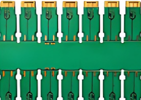
- 2 layer Rigid-Flex board
- Layer: 2L
- Board Thickness: 1.6 mm
- Surface Finishing: Immersion gold
-
- 4 layer Rigid-Flex board
- Layer: 4L
- Board Thickness: 1.6 mm
- Surface Finishing: Immersion gold
-
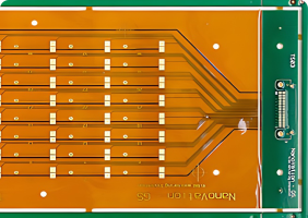
- New energy lithium battery FPC protection board
- Layer: 2L
- Board Thickness: 0.3 mm
- Surface Finishing: Immersion gold
-
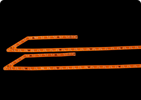
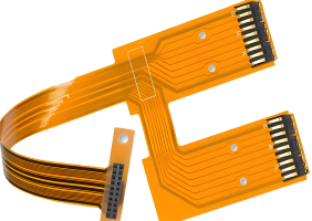
- Automotive brake light FPC board
- Layer: 2L
- Board Thickness: 0.2 mm
- Surface Finishing: OSP
-
- Aluminum-base PCB for Automotive light
- Layer: 2L
- Board Thickness: 1.0-0.2 mm
- Surface Finishing: OSP
-
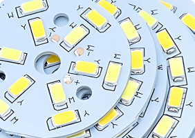
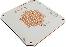
- 1 layer Aluminum-base PCB for LED light source
- Layer: 1L
- Board Thickness: 1.6 mm
-
- 2 layer copper material board
- Layer: 2L
- Board Thickness: 2.0 mm
- Surface Finishing: Immersion gold
-
- Thermal and electrical separation copper-base board
- Layer: 2L
- Board Thickness: 1.6 mm
- Surface Finishing: OSP
-
- DPC ceramics AI smart control board
- Layer: 2L
- Board Thickness: 1.0 mm
- Surface Finishing: Immersion gold
-
- 99% alumina ceramics PCB
- Layer: 2L
- Board Thickness: 1.0 mm
- Surface Finishing: ENEPIG
-
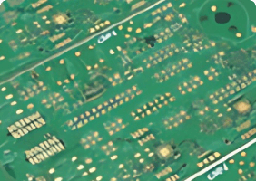
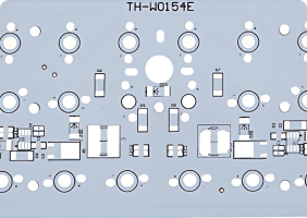
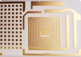
- Optical Module PCB
- Layer: 6L
- Board Thickness: 1.0 mm
- Surface Finishing: Immersion gold 5u"
-
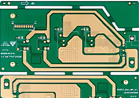
- 10 layer high frequency PCB
- Layer: 10L
- Board Thickness: 1.0±0.1 mm
- Surface Finishing: Immersion gold 2u"+ Hard gold plating …
Deep Cultivation of High Layers Count Board and Multilayer and Multi-Technology PCB production
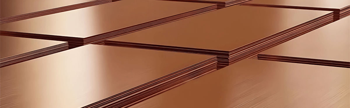
Strictly Select High Quality Raw Materials
The core material of printed circuit boards (FR-4, high TG, halogen-free, high frequency), we use brand raw material, from the source to eliminate defective products, to ensure product quality, the production process strictly in line with the international PCB quality system standards.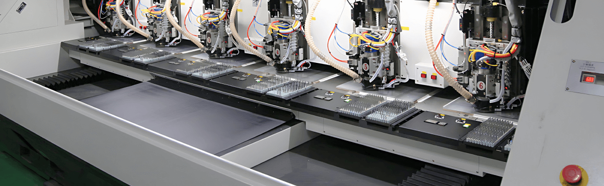
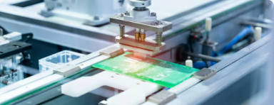
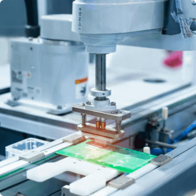
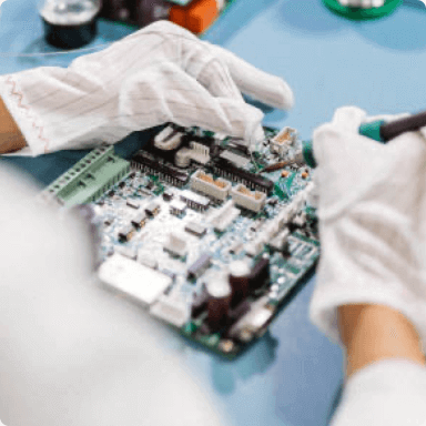
High Precision Equipment
A full set of automated production equipment, real-time data control throughout the process, effectively ensure delivery on time, to meet your R & D design demand. More equipments like laser drilling machine, automatic silkscreen printing machine, high precision etching line, copper thickness measuring instrument and etc, to ensure reliable quality.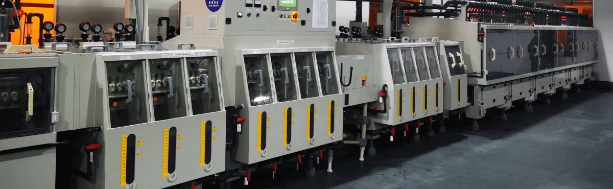
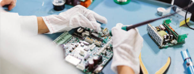
Special Process Technology
Meet all kinds of special process requirements such as HASL LF, gold plating, ENEPIG and immersion silver. The whole manufacturing process has 36 processes of layer-by-layer inspection to ensure the safety of PCB products with complete certification UL, ISO9001, IATF16949, ISO45001, ISO14001, etc, and the qualified rate of finished products is over 99%, ensuring quality priority.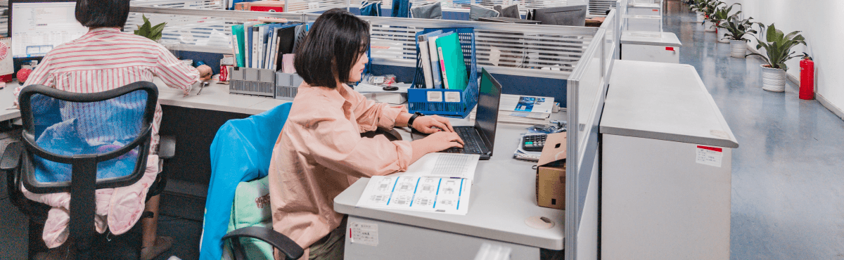
Focus on PCB Service
27 years of PCB manufacturing experience, 100+ online and offline team, accurate ERP management system and independent research and development of ICAM software from the cut lamination to the finished product shipment of all processes one-stop production, eliminating the intermediate outsourcing links, reduce costs, efficient procurement, all you have to do is wait and we will take care of the rest!High Reliability · Special Technology PCB · Manufacturer
-
Advanced Manufacturing Capabilities
Advanced Manufacturing Capabilities
Top PCB factories are equipped with modern production equipment and process technology to produce boards of all complexity, including high density interconnect (HDI) boards, flexible circuit boards (FPC) and rigid-flex boards. -
Strict Quality Control Management
Strict Quality Control Management
Our factory implement strict quality control systems, which comply with international standards such as IS09001, IS014001 and IPC, to ensure the performance stability and reliability of products, to meet customers' demands for high-quality PCBs. -

Strong R&D and Innovation Capability

Strong R&D and Innovation Capability
Leading PCB factories invest significant resources in technology R&D and innovation, keep up with the development trends of the electronics industry, and provide customized solutions to meet the changing and improving needs of customers, while driving the technological progress of the industry.
The Key Figures of Cooperative Customers
Excellent customer service to ensure your satisfaction and make us to be your preferred partner for PCB manufacturing.
-
128+
global
countries and regions delivered -
2800+
service
satisfied customers -
1000+
orders
daily orders -
95%
delivery rate
on time delivery
PCB Manufacturer choice for global customers
The Common Choice of Cooperative Customers
Contact Us